The NOT-AND operation is known as the NAND operation. Following figure shows two input NAND gate.
The standard symbol of NAND gate is shown in following diagram. Here, a bubble on the output side of the NAND gate represents NOT operation, inversion.
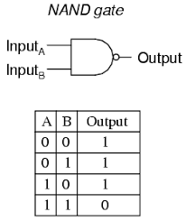
Figure shows 2-input AND gate followed by a NOT gate. The operation of this circuit can be described in the following way:
The output of the AND gate (Y') can be written as
Y' = AB .. N
Now, the output of the NOT gate (Y) can be written as
_ ________
Y = Y' = (AB ... N)
The logical operation represented by above equation is known as the NAND operation.
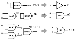
The three basic logic operations AND, OR and NOT can be performed by using only NAND gates. These are given in following figure.
The standard symbol of NAND gate is shown in following diagram. Here, a bubble on the output side of the NAND gate represents NOT operation, inversion.
Figure shows 2-input AND gate followed by a NOT gate. The operation of this circuit can be described in the following way:
The output of the AND gate (Y') can be written as
Y' = AB .. N
Now, the output of the NOT gate (Y) can be written as
_ ________
Y = Y' = (AB ... N)
The logical operation represented by above equation is known as the NAND operation.
The three basic logic operations AND, OR and NOT can be performed by using only NAND gates. These are given in following figure.
No comments:
Post a Comment